
A Short Break
Wow it’s been over a month since I last posted. I’ve mostly had life pop up recently. My birthday was on the 10th of June 🎈, so we had lots of celebrations around that. I was also waiting for my new batch of parts to reach in. I made a small mistake while ordering my parts. I thought if I ordered a big box of sensors, I would have everything I needed to practice the essentials (I2C, SPI, UART, etc.).
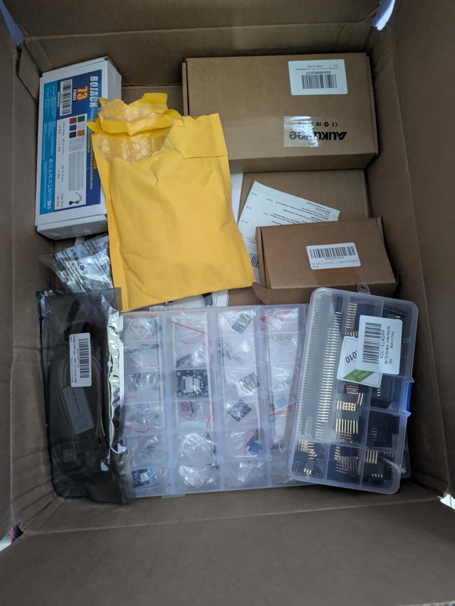
Unfortunately, I was wrong. The sensors all had a weird 3-pin system, instead of the standard SDI/SCL pins etc. for these peripherals. I guess only the more accurate sensors (and more expensive ones) have these standard protocols. I therefore picked out another batch of sensors that I confirmed were I2C, and I’m currently waiting for those to reach. The screen and SD card readers I bought should be enough to cover the basics of SPI.
In the meantime, I was spending my time watching some more videos from Dr. Miro Samek, on his Quantum Leaps YouTube channel. I stopped trying to implement everything on my STM32 board, because I found it way more interesting to watch everything and understand the base concepts that he was teaching first.
He has some great ideas on both high level design as well as low level technical concepts. I knew the basic while(1) loop architecture was weird, and he explained and criticized this ‘Superloop’ architecture well, while comparing it to event-driven and state machine architectures. He also went into real-time operating systems (RTOS), and object-oriented programming in embedded systems. It was really educational, but I felt like I was missing many of the base concepts that I really wanted to learn, so I decided to take a step back and come back to Lars’ channel. Miro is a great teacher and a really experienced developer, but I wanted to prioritize the basic, widely used concepts and protocols first, before going into the more advanced topics and the custom QP framework/solutions that he was teaching.
We started off this video by understanding the basics of the protocol using the block diagram:
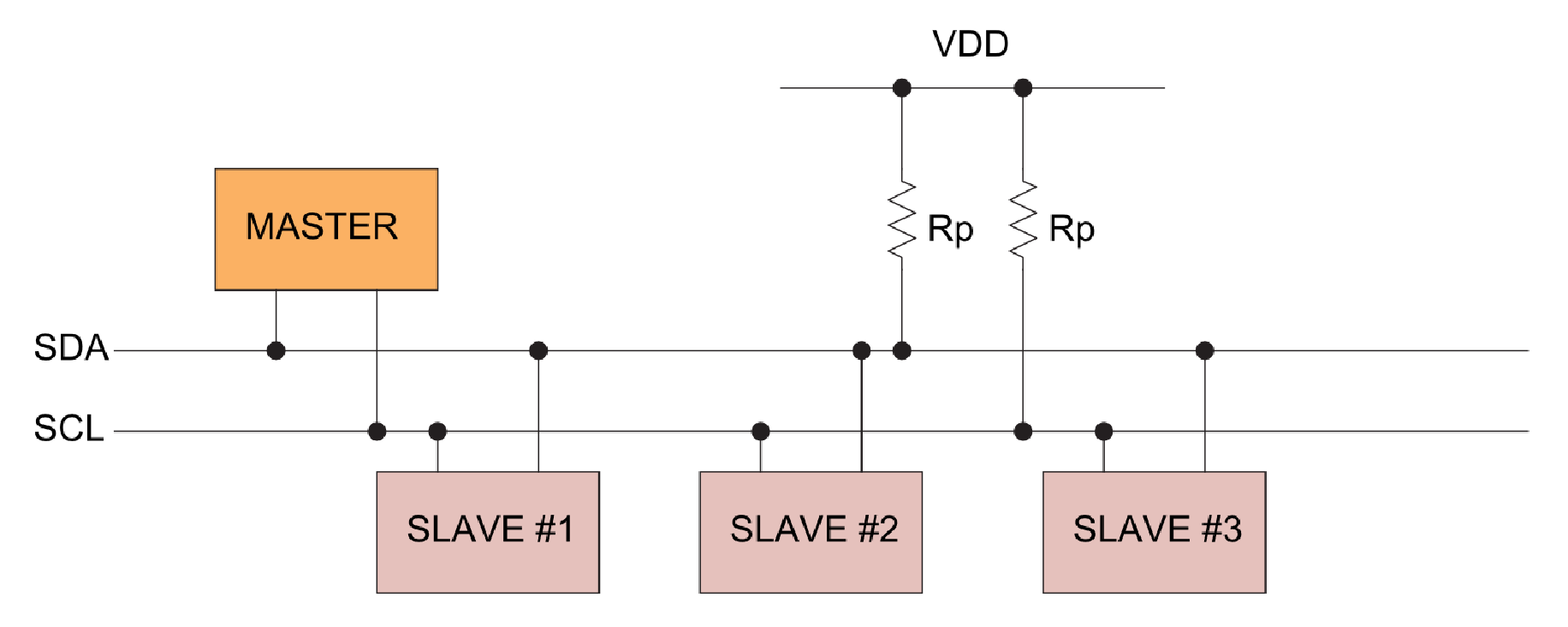
From this diagram, we can see that the I2C protocol uses two wires for communication: An SDA line (Serial Data Line) and an SCL line (Serial Clock Line). The SDA line is used to transfer data, while the SCL line is used to synchronize the data transfer between the master and slave devices. The master device generates the clock signal on the SCL line, while the slave devices respond to this clock signal. I2C is therefore a synchronous protocol.
(Images and extra details sourced from: here)
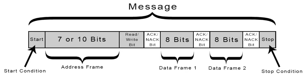
In order to communicate, the I2C master first drops the SDA line from 1 to 0, before the SCL line goes from 1 to 0. This is the start condition.
To end communications, the master raises the SDA line from 0 to 1, after the SCL line goes from 0 to 1. This is the stop condition.
After the start condition, the master sends the (normally) 7-bit address of the slave device it wants to communicate with, followed by a read/write bit (as the least significant bit). A 1 in this LSB indicates a read operation, while a 0 indicates a write operation (i.e. the master is writing to the slave). These 8 bits, as well as the subsequent data bits, are referred to as ‘frames’.
Once the receiver receives this frame successfully, it sends an ACK bit (acknowledge) by pulling the SDA line low (to 0) during the next clock cycle. A NACK bit (not acknowledge) is sent by leaving the SDA line high (to 1) during the next clock cycle.
I can’t wait to actually implement this using my new sensors. In the meantime, I might test out the ESP32 board I bought in my last order.